From www.tomshardware.com
Splitting complex chip designs into multi-chiplet solutions is all the rage these days. AMD already uses multi-chiplet designs for its CPUs and datacenter GPUs, and it also has less complex chiplets for its current generation RDNA 3 RX 7000-series GPUs. Now it looks like the company is looking to produce more complex multi-chiplet GPUs for a wider range of applications, according to a new patent filed on December 8, 2022, and discovered this week.
“A graphics processing unit (GPU) of a processing system is partitioned into multiple dies (referred to as GPU chiplets) that are configurable to collectively function and interface with an application as a single GPU in a first mode and as multiple GPUs in a second mode,” the abstract description of the patent application reads.
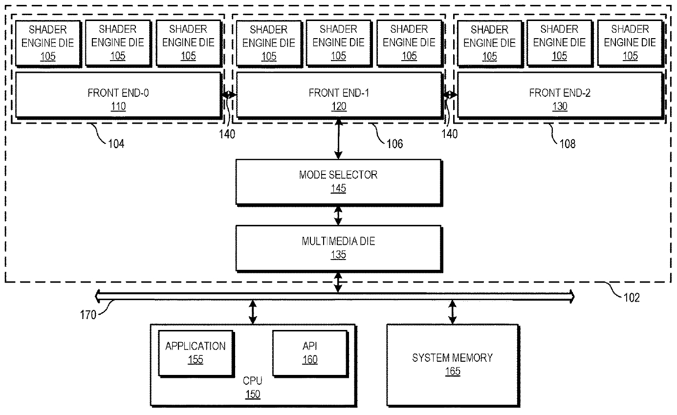
This clearly differs from the current RDNA 3 architecture, where AMD uses a central GCD (Graphics Compute Die) chiplet for all the major functions of a GPU, and multiple MCD (Memory Cache Die) chiplets for the memory interface and cache. The CDNA data center GPUs are more like what’s described here, with multiple compute/processing chiplets.
The patent describes a rather specific implementation of a GPU with three GPU chiplet sets and a multimedia die. Each GPU chiplet set consists of a front-end die and shader engine dies (the patent shows three SE dies, though the actual number could be different). Such a multi-chiplet GPU can function in three modes:
- First Mode, Single GPU: All GPU chiplets work together as a unified GPU, sharing resources and processing tasks collaboratively. In this mode, one front-end die typically handles command scheduling for all shader engine dies within the GPU. This is basically how traditional GPUs work.
- Second Mode, Multiple GPUs: The GPU chiplets are divided into distinct groups, each functioning as an independent GPU. Each group has its own front-end die responsible for scheduling tasks for its associated shader engine dies.
- Third Mode, Hybrid Configuration: This mode offers a flexible configuration where some GPU chiplets operate as a single GPU, while others function as independent GPUs.
AMD’s datacenter GPU designs have been disaggregated for several years, and the patent most likely targets multi-chiplet datacenter GPUs first, but it could also extend to client GPUs. There are several reasons why AMD may be looking to disaggregate its client GPUs in the future.
First up, with the arrival of High-NA EUV lithography and its halved exposure field (or reticle size), multi-chiplet designs will become more common in general. Given that AMD already has enough experience with multi-chiplet designs, multi-chiplet GPUs could be a viable option.
Second, as large monolithic dies are getting prohibitively expensive to tape out and produce, adopting a multi-chiplet design for client GPUs is a good way for AMD to cut down on costs. It already did this in part with the GCD/MCD chiplets, but that’s current the first iteration of client chiplets and we expect AMD to continue down that road with future designs. Chiplets also make it possible to put the shader engine and primary compute hardware on a leading-edge node, with the front-end engine on an older and cheaper process technology.
With multiple chiplets, it’s getting easier to scale GPU performance from entry-level solutions to high-end products. In fact, this is what AMD’s abstract description says:
“By dividing the GPU into multiple GPU chiplets, the processing system flexibly and cost-effectively configures an amount of active GPU physical resources based on an operating mode,” the patent claims. “In addition, a configurable number of GPU chiplets are assembled into a single GPU, such that multiple different GPUs having different numbers of GPU chiplets can be assembled using a small number of tape-outs and a multiple-die GPU can be constructed out of GPU chiplets that implement varying generations of technology.”
Again, AMD has already laid claim to using GPU chiplets with RDNA 3, but this clearly represents a step beyond that level of breaking functionality into different chips. We saw something similar with the Ryzen CPUs, where the first generation of chiplets was more of a proof of concept, with following designs better segregating functionality to extract maximum performance and scalability. AMD isn’t done with GPU chiplets, and we suspect most players in the GPU space will end up taking a similar approach.
[ For more curated Computing news, check out the main news page here]
The post AMD patents configurable multi-chiplet GPU — illustration shows three dies | Tom’s Hardware first appeared on www.tomshardware.com