From www.pcmag.com
We’ve heard plenty over the past year or two, in broad terms, about Intel’s upcoming roadmap for its silicon, its fundamental changes to its processor branding, and the new lingo (Intel 4, Intel 7) under which it will be referencing its future manufacturing processes. Here in September, Intel is peeling back another layer from the covering over its next-generation processors, code-named “Meteor Lake.”
In the old Intel world, these chips would likely have been dubbed the chip giant’s 14th Gen Core processors. But that verbiage is out, and while Intel hasn’t detailed any particulars about the names, speeds, or feeds of its first Meteor Lake chips, the company did present a wide view of its coming innovations.
Meteor Lake processors will be coming to consumer laptops first (as opposed to desktop chips), no surprise given the heavy emphasis in early briefings on efficiency and battery life savings. But Intel still hasn’t laid out its hand entirely on this new wave of processors. During a recent series of deep-dive presentations on Meteor Lake for industry and the press, dubbed Intel Tech Tour, Intel detailed new information about how the upcoming chips are made with new designs, updated technology, and fresh features that, it claims, will boost performance and efficiency going forward.
Again: Intel isn’t yet discussing specific upcoming Meteor Lake chip models, talking about first implementations, or sharing fine details about performance. But during the Tech Tour, it revealed plenty of inside-baseball information regarding Meteor Lake. The newest Intel mobile processors should feature several changes, from the manufacturing and design of the chips to the capabilities available to users. Here’s a quick overview of all the new stuff, from the silicon on up.
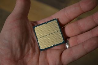
What Is Meteor Lake? Intel’s First Core Ultra Chips
We learned earlier this year that Intel chips were set up for a major re-branding, giving Intel’s Core processors simpler names and retiring the explicit generation numbers (12th Gen Core, 13th Gen Core, and so on). But Meteor Lake changes much more than just the labels. Intel revamped almost everything about the new chips, from the die layout to the architecture, adding new features, new capabilities, and a course for more innovation going forward.

(Credit: Intel)
Meteor Lake also includes changes to the manufacturing processes, introduces a reimagined “stacked” 3D design combining the parts of the CPU, and expands on the tiered high-power-vs.-low-power processor-core approach introduced in recent years. With so much going on, it’s time to reintroduce the familiar Intel processor. This processor design is behind what Intel will likely call its first generation of Intel Core Ultra processors, dropping the “i” for simplicity.
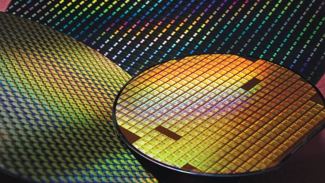
Intel 4 Manufacturing: 7nm Is Finally Here
Intel’s biggest upgrade is at the foundry level, moving to what it is now calling its Intel 4 process. This new 7-nanometer (7nm) manufacturing process uses extreme ultraviolet (EUV) lithography, a chip-making method that allows for ever-smaller chips, keeping Moore’s Law chugging along with tinier—and therefore more, in a given surface area—transistors.
The EUV lithography equipment that Intel uses may be the most complicated machinery ever made, by the chip maker’s own claim, but the benefits are easier to understand: better scaling and boosted power efficiency. Compared with the previous 10nm Intel 7 process, Intel 4 is expected to deliver 20% better performance per watt.
It’s also optimized for high-performance applications, supporting both low- and high-voltage operations, giving the CPUs greater flexibility in handling different processes efficiently.
Foveros 3D Die Stacking: Monolith No More
Foveros is Intel’s new packaging technology, which uses 3D stacking to combine multiple component tiles (sometimes called “chiplets”) into a single chip. This lets Intel use a disaggregated design (more on what that is in a moment), which is more customizable than previous methods that made CPUs as a single slab or “monolith.”

(Credit: Intel)
The move away from monolithic design means that Intel can now customize each part of the processor separately, optimizing for specific functions and assembling the pieces into a small, efficient 3D stack. It also means that different production methods can be used for different parts of the chip. Intel can opt to manufacture the central processing portion using its latest (for now, Intel 4) approach, while it can continue using older processes for other sections of the final assembled chip (letting Intel leverage existing manufacturing lines and technologies), or even farm out portions to other manufacturers altogether.
Another key aspect of the process improvement? For Intel, it lets the company precisely assemble the processors from pre-tested components, instead of “binning” the entire assembled CPU after fabrication. Binning is the process of separating out and categorizing finished CPUs based on how many components in a given sample fail to meet the fabricator’s highest standard for that current architecture.
Components that don’t quite make the grade are packaged as “lesser” versions based on those imperfections. Binning is how you get the different power tiers of processors, which will now likely be known as Intel 9, Intel 7, Intel 5, and so on. Top-tier samples in testing end up as “9” level chips, all the way down.
In this new tiled-component model, Intel can assemble its CPUs from parts that are already tested. This also makes future feature development easier, as the company can update individual portions of the overall chip without a full redesign of an entire “single piece” monolithic processor being necessary.

(Credit: Intel)
Now, all of that may sound great in theory, but the tiles need to talk to each other, and at blink speed. Joining all of these tiles together requires special die-to-die interconnects, the literal micro-wires that link different sections of the CPU for I/O, power delivery, and die-to-die routing. That is where the company’s Foveros technology comes in. Foveros uses high-density, high-bandwidth, and low-power interconnects, unifying the different parts of the design.
It’s not an entirely new approach—AMD has employed chiplet designs for years now—but it’s a big shift for Intel that will play a huge role in how the company makes its processor hardware going forward.
Intel’s Tile Layout and Disaggregated Design: Breaking It Down
This new tile-based approach is a type of disaggregated design. Instead of designing a single monolithic chip, the CPU can be built out of smaller, simpler parts, and assembled onto a base wafer, fusing them together into a single chip die using those aforementioned interconnects. But this Voltron-like approach requires several different pieces all working together.
Meteor Lake will use four distinct tiles, with each dedicated to the different technologies used in modern processors: Compute, Graphics, SoC, and I/O.
The Compute Tile
The heart of the Meteor Lake chip is what most folks think of in the classic sense when discussing processors. The Compute Tile contains the Performance cores (P-cores) and Efficient cores (E-cores) that do the heavy lifting for your system. Built on the latest 7nm Intel 4 process, this is the most advanced tile of the four.

(Credit: Intel)
Intel’s P-cores now have a new microarchitecture that the chip maker is dubbing “Rosewood Cove.” The E-cores, meanwhile, have been updated with a microarchitecture called “Crestmont.” Specific advancements have been made to enhance multi-threaded workloads, increase cache and memory bandwidth, and provide acceleration for AI workloads.
Thread Director is a key component to all of this. This firmware, built into the hardware and a feature of previous gen Intel chips, makes sure that the processing tasks in play are being shunted to the optimal core at the right time. With Meteor Lake, an improved Thread Director ties these cores together with better task-scheduling capabilities and improved guidance, shunting less-demanding tasks to the E-cores, or to the new “Low Power E-cores” found on the SoC tile (more on them in a moment) for efficiency and power savings.
That on-the-fly prioritization reserves the P-cores for higher-demand tasks, and it can lead to power savings, because at times, the Compute Tile may not need to be spun up at all. Intel also co-designed the new version of Thread Director with Microsoft to tailor it closely to Windows 11, for tighter integration between the hardware and software.
SoC Tile
The SoC Tile is something of a catch-all, encompassing functions such as basic media and display control, Wi-Fi connectivity, and hardware security. But it also has a new, special zone.

(Credit: Intel)
A dedicated area of the SoC Tile, which Intel dubbed the “Low Power Island” in its briefings, provides an isolated cluster of additional efficient processing cores: the Low Power E-cores mentioned above. As the name suggests, these cores are optimized for handling low-lift workloads and background processes, delivering better efficiency and reserving the cores on the Compute Tile for more demanding application processes.
Recommended by Our Editors
In addition, because the Low Power Island can be power-managed separately from the higher-performance cores, it eliminates some of the power overhead that occurs in current CPUs. If a set of tasks doesn’t need to employ the P-cores or E-cores on the Compute Tile at all, that can lead to power savings by leaving that Tile dormant for a time, while all the action occurs on the Island.

(Credit: Intel)
The SOC Tile also includes Intel’s first integrated artificial intelligence engine, a neural processing unit (NPU) specifically for running local, client-side AI models efficiently. (In earlier discussions around Meteor Lake. the NPU was also variously being referred to as a “VPU.”) The NPU works cooperatively with the CPU to handle AI workloads. Intel put it on the SoC tile in order to provide high-bandwidth access to other portions of the chip, allowing AI to enhance everything from graphics to Wi-Fi performance. (Read more about the NPU in Meteor Lake in this side article.)

(Credit: Intel)
Speaking of other functions, the SoC Tile includes display and media support, with native HDMI 2.1 and DisplayPort 2.1 built-in, as well as 8K HDR content support and advanced AV1 codecs. This tile also manages Wi-Fi connectivity, with support for current Wi-Fi 6E and upcoming Wi-Fi 7 networking.
The SoC Tile is also home to the memory controller and the double data rate (DDR) bus for communicating with system memory.
Graphics Tile
The third tile, the Graphics Tile, handles all of the graphics and compute workloads for gaming, content creation, and some of the media streaming. Here, Intel flexes one of its other new technology product lines: Intel Arc. This tile integrates the Arc graphics technology, in this environment known as Alchemist Xe LPG, directly into the CPU Graphics Tile. (Hit the link for lots more on Meteor Lake’s new on-chip Arc graphics.)

(Credit: Intel)
The result will level up the muscle and capability of Intel’s integrated graphics support considerably. This Arc-level performance won’t be available on all Meteor Lake chips, but Intel will now provide integrated graphics above and beyond its Iris Xe solution of today.
I/O Tile
This last portion of the chip is all about connectivity, handling all of the pins and signaling from external connections. These traditionally include connections like USB and storage, and Intel specified that the new platform integrates standards like Thunderbolt 4 and PCI Express Gen 5.

(Credit: Intel)
Though Intel didn’t directly say so, we suspect Thunderbolt 5 support may be baked in as well. Intel claimed (in a separate briefing specifically on Thunderbolt 5) that the new Thunderbolt standard would launch in 2024. It may be a bit premature for Intel to include the new standard on the first wave of upcoming Meteor Lake chips. But it wouldn’t surprise us if Thunderbolt 5 gets mentioned again when Meteor Lake machines are announced in the future.
Intel’s Chiplet-Shaped Comeback Is Coming
Intel has faced competitive pressure on all sides in recent years, from AMD to Apple (with Arm) and other mobile chip makers at most levels of the market for laptops and desktops. Meteor Lake isn’t just an iteration on past generations of Intel’s Core processors, but a major shift in both process and philosophy to stay competitive in the years to come.
With Intel’s vendor partners already in the know (and certainly hard at work integrating the first Meteor Lake processors into upcoming system designs), this announcement signifies to consumers that more powerful and versatile Intel-based laptops are on the horizon, likely following this holiday season.
We don’t know exactly when these new CPUs will show up in new laptops, though Intel has confirmed that the new Core Ultra chips will launch December 14. With CES 2024 around the corner, and Thunderbolt 5 slated for 2024 as well, early next year seems a solid guess for Meteor Lake’s first streak across the sky as OEMs start to announce Meteor Lake-based machines. We’ll have coverage as new details emerge and the first Meteor Lake-equipped laptops are announced. More Meteor soon.
Get Our Best Stories!
Sign up for What’s New Now to get our top stories delivered to your inbox every morning.
This newsletter may contain advertising, deals, or affiliate links. Subscribing to a newsletter indicates your consent to our Terms of Use and Privacy Policy. You may unsubscribe from the newsletters at any time.
[ For more curated Computing news, check out the main news page here]
The post ‘Meteor Lake’ Architecture Detailed: What to Know About Intel’s Next-Gen CPUs first appeared on www.pcmag.com