From www.techspot.com
Serving tech enthusiasts for over 25 years.
TechSpot means tech analysis and advice you can trust.
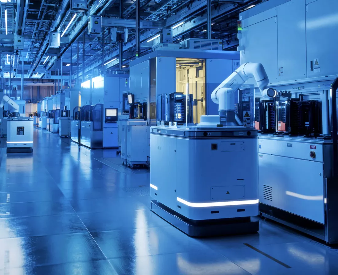
What just happened? TSMC has challenged Intel’s claims that it will overtake the Taiwanese company when it comes to making the world’s fastest computing chips by unveiling its A16 (1.6nm) manufacturing process. TSMC says the massive demand from unnamed AI customers meant the A16 technology has been developed faster than expected.
A16, set to enter production in the second half of 2026, will use leading nanosheet transistors and what TSMC calls an “innovative” backside power rail solution to bring “revolutionary performance” to the wafer level. While traditional chip designs involve power flowing from the top down, the backside power rail system delivers power from the bottom. The company writes that this will help address future AI requirements for hyperscale datacenters.
Intel says it also plans to integrate backside power rail technology into its 20A (2nm) and 18A (1.8nm) processes as early as 2025.
According to TSMC’s roadmap, its 2nm N2 process node is on track for production in the second half of 2025, the successor to its 3nm N3E technology that is now in production. A16 will follow in 2026, combining TSMC’s Super Power Rail architecture with its nanosheet transistors. It improves logic density by dedicating front-side routing resources to signals, which should make it ideal for HPC products. Compared to N2P, A16 will provide an 8-10% speed improvement, 15-20% power reduction, and up to 1.10x chip density improvement.
Kevin Zhang, TSMC’s senior vice president of business development, said the company doesn’t believe it will need to use ASML’s new High NA EUV lithography tool machines for the A16 process.
Intel said last week that it will be the first to use ASML’s machines, which cost $373 million each, to help develop its 14A (1.4nm) chips. Team Blue said in February that 14A would help it overtake TSMC in making the world’s fastest chips. Samsung, meanwhile, is aiming to mass produce its 1.4nm chips by 2027.
Intel’s foundry business lost $7 billion last year, something CEO Pat Gelsinger put down to past mistakes, including the decision to not use ASML’s EUV machines. Intel later went back on its decision and invested in the EUV machines, which should help the foundry business’ goal to break even in about three years.
TSMC emphasized the benefits the A16 process will bring to AI chip makers. Zhang said these firms “really want to optimize their designs to get every ounce of performance we have.” Earlier this year, TSMC founder Morris Chang predicted that up to 10 new fabs would be required for AI chip manufacturing.
[ For more curated Computing news, check out the main news page here]
The post TSMC unveils A16 manufacturing process for 1.6nm chips in challenge to Intel’s claims first appeared on www.techspot.com


/cdn.vox-cdn.com/uploads/chorus_asset/file/25546355/intel_13900k_tomwarren__2_.jpg "There is no fix for Intel’s crashing 13th and 14th Gen CPUs — any damage is permanent")


